


Next: PLL Tracking
Up: Performance Comparison of Different
Previous: Performance Comparison of Different
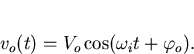
In this section the ability of a phaselock loop to cope with noise is examined. Consider the input signal of a phaselock loop and assume that as well as a sinusoidal signal, additive noise of n(t)volts with one sided spectral density Sn(f) is also admitted. Therefore the input voltage to the phase detector is given by
![\begin{displaymath}
v_i(t)=V_s\sin(\omega_it+\varphi_i)+n(t)\quad [V].\end{displaymath}](img108.gif)
The other input to the phase detector is due to the VCO. Because it is typical that VCO's lock in quadrature to the incoming signal, the VCO signal is typically  out of phase with vi. In anticipation of this fact, it is useful to write
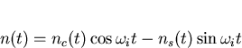
The additive noise n(t) can be expanded into two quadrature components
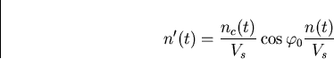
One may then define the dimensionless quantity n' as
It can be shown [11] that the variance,  of the output noise n(t) is given by
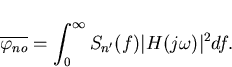
where  is the filter transfer function defined by equation (3.13), Sn'(f) is the one-sided spectral density of n' and
  .
In general, the form of Sn(f) impedes the evaluation of the above integral. If one considers white noise where
.
In general, the form of Sn(f) impedes the evaluation of the above integral. If one considers white noise where  , the above integral simplifies to
where
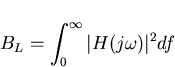
is the noise bandwidth .
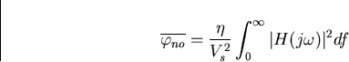
Hence for input white noise, the phase variance is simply
| 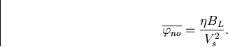 |
(21) |
Gardner [11] details the noise bandwidths of various loop types and they are reproduced in table 3.3.
Table 3.3:
Noise bandwidths of common loops
| Loop Description |
Noise Bandwidth, BL(Hz)) |
| First Order |
 |
| Second order passive |
 |
| Second order active |
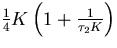 |
where K is the open loop gain defined for various loops in table 3.2. It can be seen that K plays a central role in establishing the noise bandwidth and hence the output phase variance. It is necessary for K and hence KoKd, to be small in order to minimise the output jitter due to external noise.
Next: PLL Tracking
Up: Performance Comparison of Different
Previous: Performance Comparison of Different
Mark J Ivens
11/13/1997