


Next: Filter Transfer Functions and
Up: Phaselock Loops
Previous: Basic PLL Components
In this section elementary mathematical analysis of a simple phaselock loop is performed in order to obtain the phaselock loop transfer function.
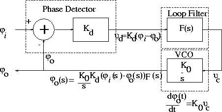
The basic phaselock loop components are shown again in figure 3.2. Further to the discussion in section 3.4.1, the function of a phase detector is to produce an output voltage proportional to difference in phase between its inputs. Thus the phase detector output voltage, vd is given by
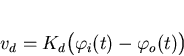
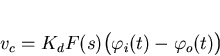
where Kd is the phase-detector gain factor measured in volts/radian. The phase detector output voltage vd then passes through the loop filter. The voltage at the output of the loop filter is given by
vc=vdF(s)
i.e.
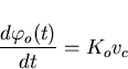
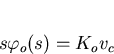
The deviation of the VCO from its centre frequency is given by
|  |
(15) |
where Ko is the VCO gain factor which has units rad/sec-V.
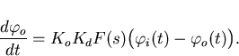
Substituting for vc yields
Taking the Laplace transform on both sides of (3.11) and using
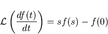
gives
which on substituting for vc becomes
| 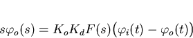 |
(16) |
Equation (3.12) may be easily rearranged to obtain the closed loop transfer function
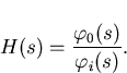
Performing such a manipulation yields the expression
| 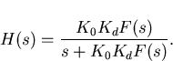 |
(17) |
It can be seen from the form of the equation that PLL's essentially low pass filter incoming signals.
Figure 3.2:
PLL block schematic
 |
Next: Filter Transfer Functions and
Up: Phaselock Loops
Previous: Basic PLL Components
Mark J Ivens
11/13/1997