


Next: One Possible Interpretation of
Up: Relationship between ETSI and
Previous: Power Spectral Densities of
Now consider the PLL block schematic in figure 5.3.
Figure 5.3:
PLL Block schematic
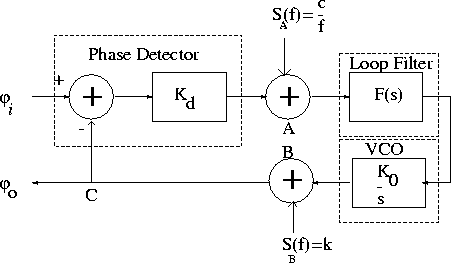 |
Assume that purely flicker phase noise is generated at point A at the output of the phase detector and that only white phase noise is generated at point B at the VCO output:
where c and k are constants. Since it will be assumed that the noise is small compared to the useful signal, superposition may be used. Now the transfer functions between the points A and B and the output are
where Kd is the phase-detector gain factor measured in volts/radian, K0 is the VCO gain factor measured in rad/sec-V and F(s) is the transfer function of the loop filter.
Using the relationship (5.2) the Power Spectral Density of SA(f) at the PLL output is
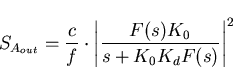
which can be simplified to
| 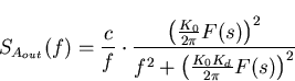 |
(40) |
Next: One Possible Interpretation of
Up: Relationship between ETSI and
Previous: Power Spectral Densities of
Mark J Ivens
11/13/1997